LVDS PCB Layout – Expert Guidelines You Need to Know! A detailed guide to pcb layout design
If you are looking for LVDS: High Speed LVDS PCB Design Guidelines | MADPCB you've visit to the right page. We have 25 Pictures about LVDS: High Speed LVDS PCB Design Guidelines | MADPCB like LVDS: High Speed LVDS PCB Design Guidelines | MADPCB, FPGA - DAC LVDS 1.25GBPS PCB SKEW IMAGE - YouTube and also LVDS to LVDS converter is to LVDS interface to LVDS interface. Here it is:
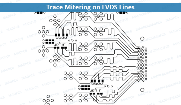
LVDS: High Speed LVDS PCB Design Guidelines | MADPCB
 madpcb.com
LVDS: High Speed LVDS PCB Design Guidelines | MADPCB
LVDS: High Speed LVDS PCB Design Guidelines | MADPCB
 madpcb.com
LVDS: High Speed LVDS PCB Design Guidelines | MADPCB
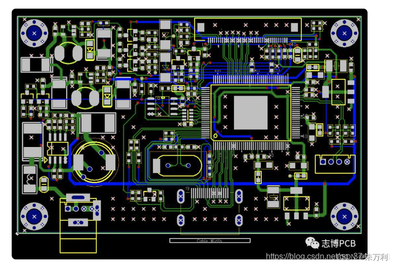
PCB模块化设计12——LVDS高速PCB布局布线设计规范_22pin接口模块设计-CSDN博客
 blog.csdn.net
PCB模块化设计12——LVDS高速PCB布局布线设计规范_22pin接口模块设计-CSDN博客
Understanding LVDS Interface: A Comprehensive Guide
 www.shiningltd.com
Understanding LVDS Interface: A Comprehensive Guide
Top 5 PCB Design Rules You Need To Know | PCB Design Blog | Altium
 resources.altium.com
Top 5 PCB Design Rules You Need to Know | PCB Design Blog | Altium
Main Design Guidelines & Layout Rules On High Speed PCB
 www.integrasources.com
Main Design Guidelines & Layout Rules on High Speed PCB
Some LVDS PCB Layout Guidelines For Ensuring Signal Integrity | PCB
 resources.altium.com
Some LVDS PCB Layout Guidelines for Ensuring Signal Integrity | PCB ...
PCB Design And Layout - Checklist Of What You Need Before You Start
 www.slideshare.net
PCB Design and Layout - Checklist of What You Need Before You Start
Some LVDS PCB Layout Guidelines For Ensuring Signal Integrity | PCB
Some LVDS PCB Layout Guidelines for Ensuring Signal Integrity | PCB ...
PCB模块化设计12——LVDS高速PCB布局布线设计规范_22pin接口模块设计-CSDN博客
 blog.csdn.net
PCB模块化设计12——LVDS高速PCB布局布线设计规范_22pin接口模块设计-CSDN博客
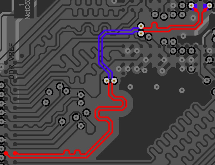
LVDS高速PCB布局布线设计_lvds等长差多少mil-CSDN博客
 blog.csdn.net
LVDS高速PCB布局布线设计_lvds等长差多少mil-CSDN博客
A Detailed Guide To PCB Layout Design - IBE Electronics
 www.pcbaaa.com
A detailed guide to PCB layout design - IBE Electronics
FPGA - DAC LVDS 1.25GBPS PCB SKEW IMAGE - YouTube
 www.youtube.com
FPGA - DAC LVDS 1.25GBPS PCB SKEW IMAGE - YouTube
LVDS To LVDS Converter Is To LVDS Interface To LVDS Interface
 lcddisplay.co
LVDS to LVDS converter is to LVDS interface to LVDS interface ...
Understanding LVDS Interface: A Comprehensive Guide
 www.shiningltd.com
Understanding LVDS Interface: A Comprehensive Guide
13 Basic Rules Of PCB Layout - Printed Circuit Board Manufacturing
 www.raypcb.com
13 Basic Rules Of PCB Layout - Printed Circuit Board Manufacturing ...
LVDS: High Speed LVDS PCB Design Guidelines | MADPCB
 madpcb.com
LVDS: High Speed LVDS PCB Design Guidelines | MADPCB
A Detailed Guide To PCB Layout Design - IBE Electronics
 www.pcbaaa.com
A detailed guide to PCB layout design - IBE Electronics
PCB Design Review: DPI-LVDS Sony Vaio LCD Devboard | Hackaday
 hackaday.com
PCB Design Review: DPI-LVDS Sony Vaio LCD Devboard | Hackaday
Understanding LVDS Interface: A Comprehensive Guide
 www.shiningltd.com
Understanding LVDS Interface: A Comprehensive Guide
Lvds Interface Conversion To Mipi Interface, Resolution Up To 1920x1200
 lcddisplay.co
lvds interface conversion to mipi interface, resolution up to 1920x1200
PCB Trace Length Matching Guidelines - TechSparks
 www.tech-sparks.com
PCB Trace Length Matching Guidelines - TechSparks
Top PCB Design Guidelines Every PCB Designer Needs To Know | Altium
 www.pinterest.co.uk
Top PCB Design Guidelines Every PCB Designer Needs to Know | Altium ...
LVDS: High Speed LVDS PCB Design Guidelines | MADPCB
 madpcb.com
LVDS: High Speed LVDS PCB Design Guidelines | MADPCB
Some LVDS PCB Layout Guidelines For Ensuring Signal Integrity | PCB
Some LVDS PCB Layout Guidelines for Ensuring Signal Integrity | PCB ...
lvds: high speed lvds pcb design guidelines. Some lvds pcb layout guidelines for ensuring signal integrity. Understanding lvds interface: a comprehensive guide