KiCad Scale Footprint: Precision PCB Design Made Simple! 08 precision assurance: performing footprint check & integrating ...
If you are searching about How to Get Your KiCad PCB Design Ready for Fabrication - KiCad Version you've visit to the right page. We have 25 Pictures about How to Get Your KiCad PCB Design Ready for Fabrication - KiCad Version like KiCad - Schematic Capture & PCB Design Software, Kicad Scale Footprint - Scrollity and also How To Make Pcb With Kicad Pcb Designs - Vrogue. Here it is:
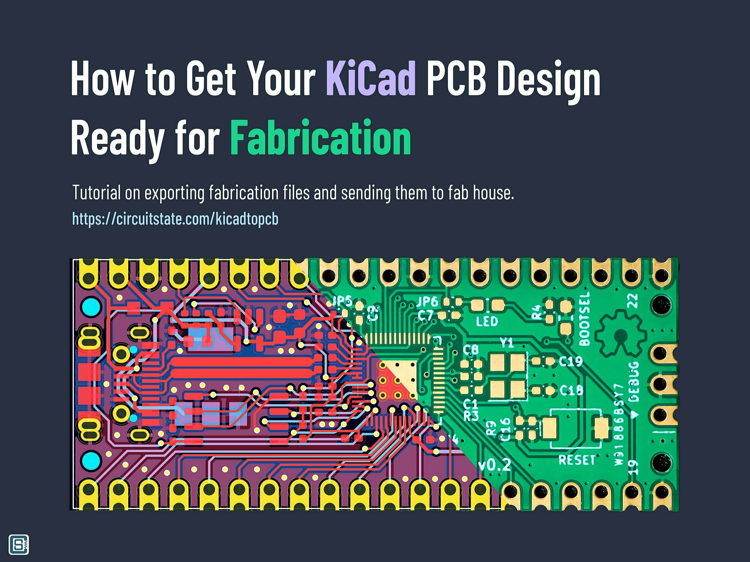
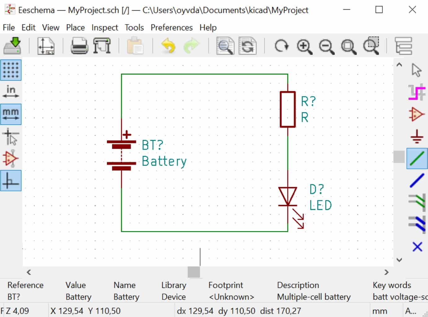
How To Get Your KiCad PCB Design Ready For Fabrication - KiCad Version
 circuitstate.com
How to Get Your KiCad PCB Design Ready for Fabrication - KiCad Version ...
KiCad PCB Design For Beginners = Kickstarter - YouTube
 www.youtube.com
KiCad PCB Design for beginners = kickstarter - YouTube
Kicad How To Make A Footprint At Kelly Duppstadt Blog
 storage.googleapis.com
Kicad How To Make A Footprint at Kelly Duppstadt blog
Documentation | KiCad
 docs.kicad.org
Documentation | KiCad
KiCad 6.0.0 Release | KiCad EDA
 www.kicad.org
KiCad 6.0.0 Release | KiCad EDA
4-Layer PCB Design In KiCad 5: Quick Thoughts | Paul Bupe, Jr
 paulbupejr.com
4-Layer PCB Design in KiCad 5: Quick Thoughts | Paul Bupe, Jr
Create Connector Footprint: Kicad Tutorial 1. 7 - YouTube
 www.youtube.com
Create Connector Footprint: Kicad Tutorial 1. 7 - YouTube
KiCad Tutorial: Make Your First Printed Circuit Board
 www.build-electronic-circuits.com
KiCad Tutorial: Make Your First Printed Circuit Board
MITAYI Pico RP2040 R0.2 - Open-source Microcontroller Development Board
 www.circuitstate.com
MITAYI Pico RP2040 r0.2 - Open-source Microcontroller Development Board ...
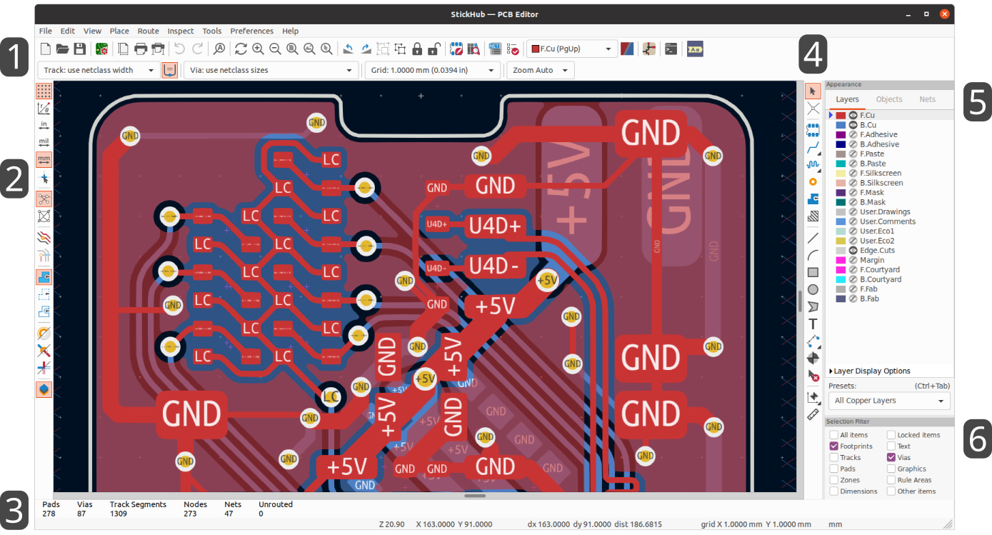
How To Make Pcb With Kicad Pcb Designs - Vrogue
 www.vrogue.co
How To Make Pcb With Kicad Pcb Designs - Vrogue
Little-scale: Kicad Footprint Library For PS4 Joystick
 little-scale.blogspot.com
little-scale: Kicad Footprint Library for PS4 Joystick
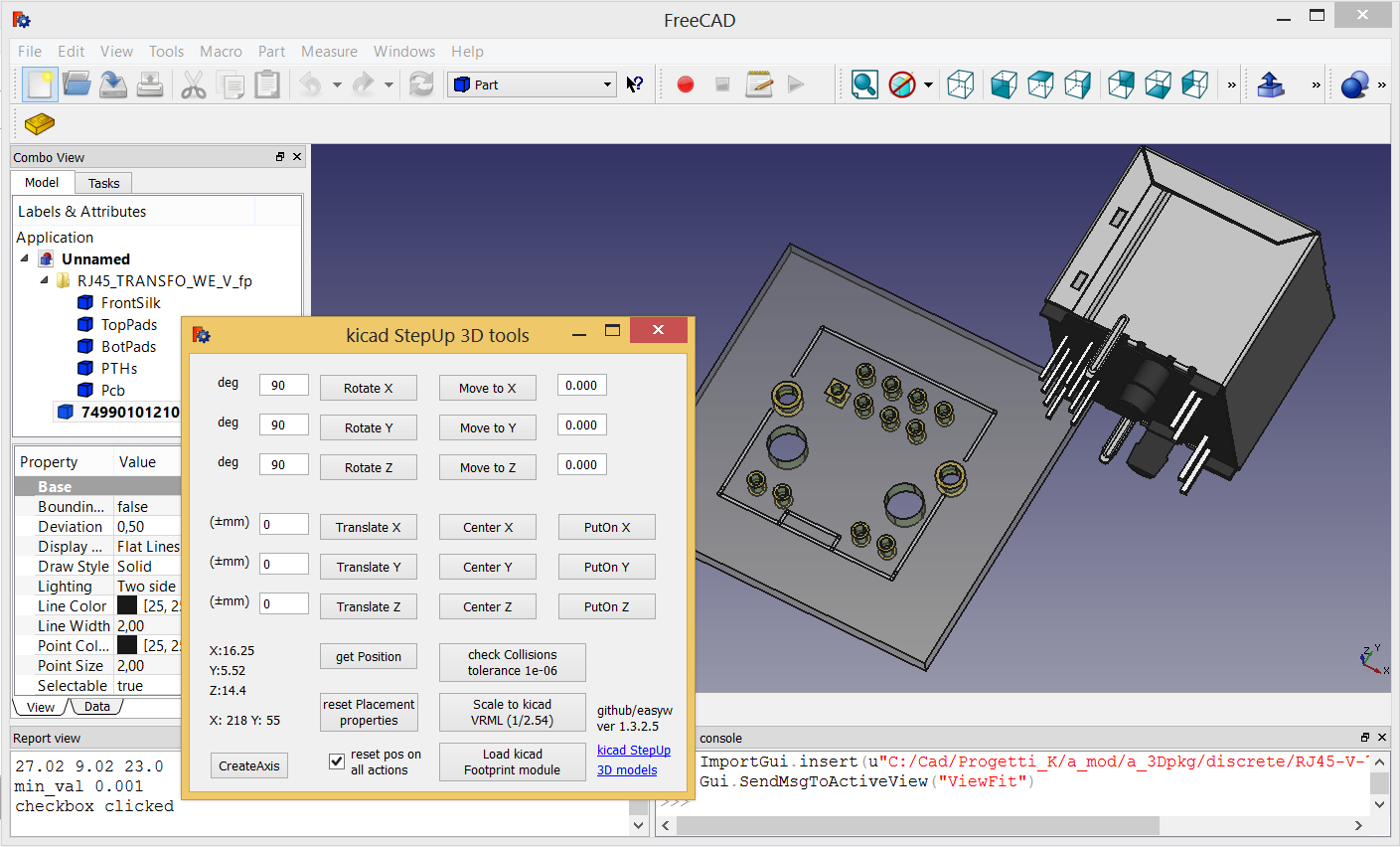
Kicad New Tool: Import 3D Model Into Footprint In Altium Style
 www.olimex.com
kicad new tool: import 3D model into footprint in Altium style
PCB Design With KiCad - YouTube
 www.youtube.com
PCB Design with KiCad - YouTube
Pcb Design Kicad Tutorial 4 Layer Pcb Design Tutorial Kicad Pcb Designs
 eroppa.com
Pcb Design Kicad Tutorial 4 Layer Pcb Design Tutorial Kicad Pcb Designs ...
KiCad PCB Design Specialist | Upwork
 www.upwork.com
KiCad PCB Design Specialist | Upwork
Kicad Update Pcb From Schematic Greyed Out Introduction To B
 circuitnghyplysu057.z21.web.core.windows.net
Kicad Update Pcb From Schematic Greyed Out Introduction To B
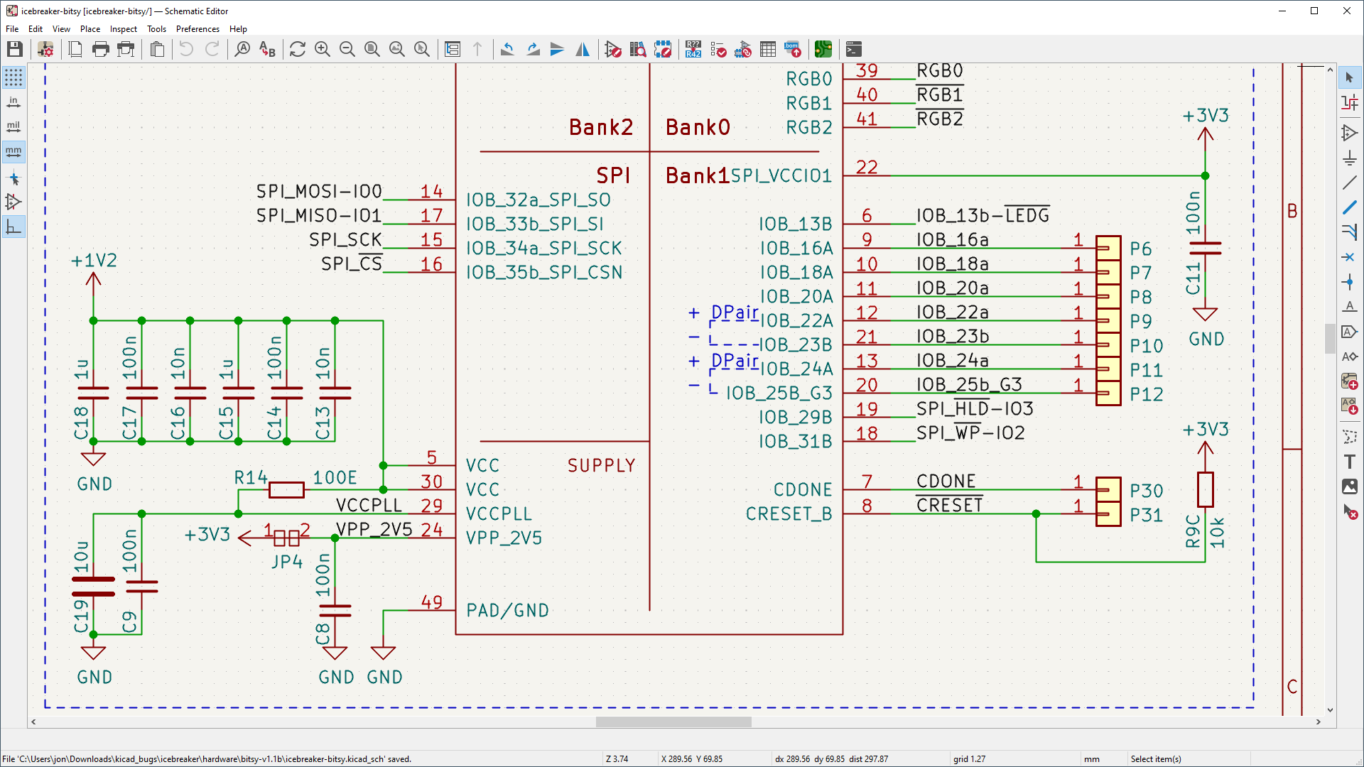
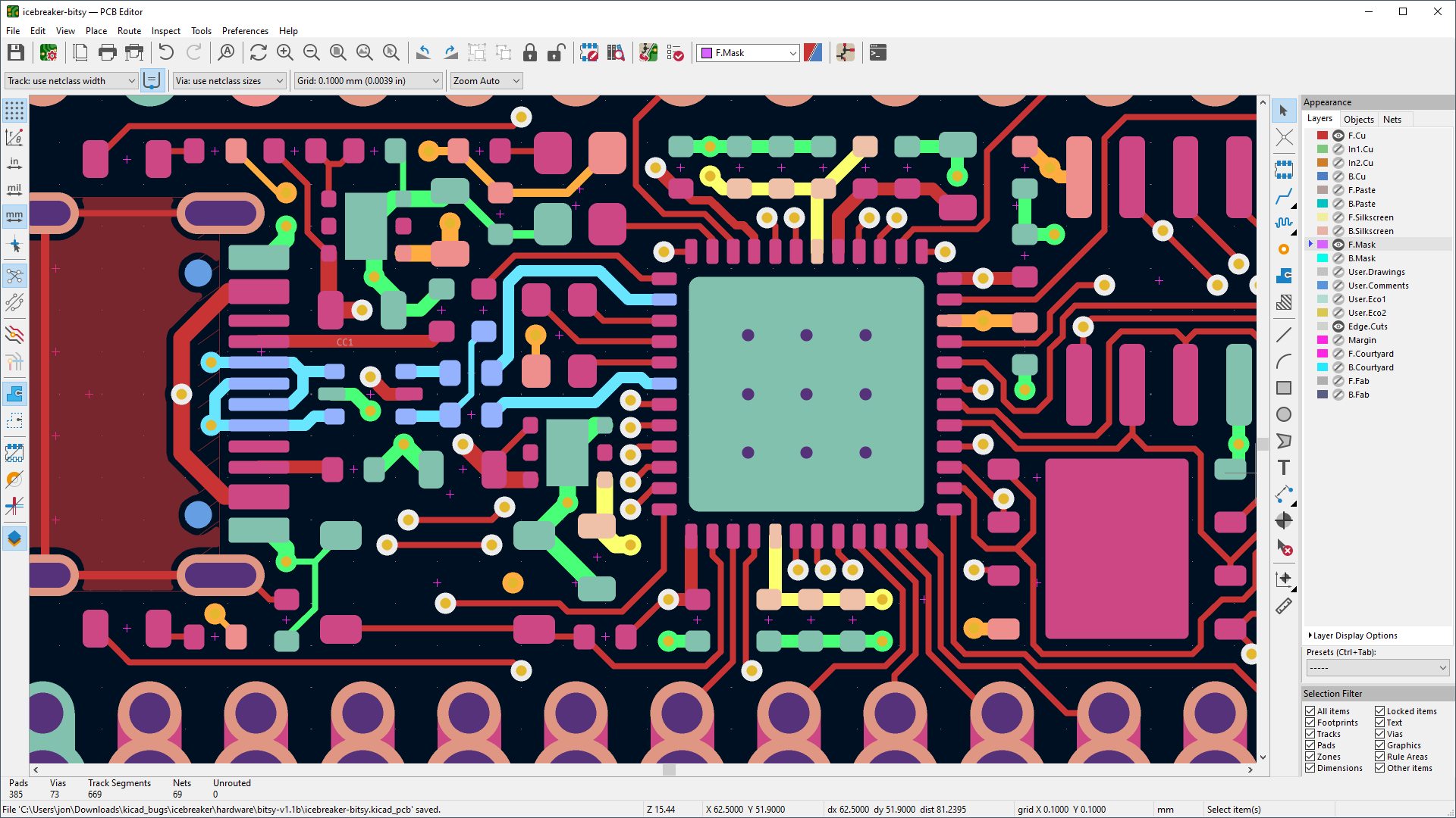
KiCad - Schematic Capture & PCB Design Software
 kicad.org
KiCad - Schematic Capture & PCB Design Software
Kicad 2 Layer PCB Design: Tips And Best Practices – Hillman Curtis
 hillmancurtis.com
Kicad 2 Layer PCB Design: Tips and Best Practices – Hillman Curtis ...
PCB Editor | Master | English | Documentation | KiCad
 docs.kicad.org
PCB Editor | master | English | Documentation | KiCad
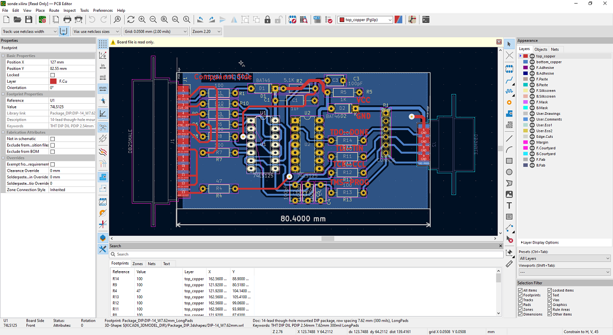
PCB Board Measurement Precision And Component Placement - Layout
 forum.kicad.info
PCB board measurement precision and component placement - Layout ...
How To Make Pcb With Kicad Pcb Designs - Vrogue
 www.vrogue.co
How To Make Pcb With Kicad Pcb Designs - Vrogue
KiCad - Schematic Capture & PCB Design Software
 kicad.io
KiCad - Schematic Capture & PCB Design Software
08 Precision Assurance: Performing Footprint Check & Integrating
 www.youtube.com
08 Precision Assurance: Performing Footprint Check & Integrating ...
My Journey From Eagle To KiCad For PCB Design | Kai Christian Bader
 www.kaibader.de
My Journey from Eagle to KiCad for PCB Design | Kai Christian Bader
Kicad Scale Footprint - Scrollity
 scrollity4.blogspot.com
Kicad Scale Footprint - Scrollity
My journey from eagle to kicad for pcb design. pcb design with kicad. Pcb board measurement precision and component placement